Paving the way for terabits per second
Increasing digitization and the corresponding security requirement, smart industry and the enormous growth of cloud applications and data centers are generating a growing need for high data speeds. Other trends are feeding the appetite for bandwidth, too, like more online communication and remote working. But the limits of what’s physically possible are coming in sight and there’s no bending the laws of nature. How do we protect signal integrity and yet realize high speeds – and all this within acceptable project budgets?
Data transfer begins and ends with electricity
By far the best way to transfer large quantities of data is with light. Communication through fiber-optic cables can achieve dazzling speeds, up to hundreds of terabits per second in test situations, and the energy loss in glass fibers is minimal. While light is the ideal vehicle for data, data journeys always begin and end with electricity – dozens of centimeters of PCB traces, with bumps and transitions. This is where the bandwidth bottleneck is situated.
Terabit Ethernet
Ethernet standards above 100 Gbit/s are usually referred to as “terabit Ethernet.” These bit rates are the product of three factors: baud rate, bit stacking and multiple lanes. To draw a comparison: a freight truck full of paper printed on both sides would contain approximately 25 billion digits. If it travels at 160 km/h, a truck passes every second: a baud rate of 25 Gbaud. By using not just the digits 0 and 1 (NRZ) but also 2 and 3 (PAM4), we can transmit two bits at the same time: 50 Gbit/s per lane. An eight-lane highway can then facilitate 400 Gbit/s in total – currently the fastest Ethernet standard.
High-speed data transfer across electrical connections faces many challenges. Ideally, zeros and ones are transmitted by sending low and high voltage pulses, respectively, across a copper trace and the same voltage appears at the end of the trace so that the information arrives in good order. In reality, things are more complicated. The faster the bits follow each other, the more the signal begins to behave like an electromagnetic wave. Bends, changes of layers and connectors cause echoes or reflections, as a result of which successive bits begin to interfere with each other. The rapid voltage fluctuations for the zeros and ones are partially lost in the form of heat, and they may also interfere with adjacent transmissions due to crosstalk. These effects all make it more difficult for the receiver to distinguish between zeros and ones. The combination of these (and other) features constitutes the signal integrity (SI) of a connection.
Designing a high-speed system affects SI in many ways, both positively and negatively. The length, shape and distance between circuits, the connectors used, the mix of serial and parallel, and the quality of the power supply (power integrity or PI) all play a role. Not to mention environmental factors during use, such as temperature (the system itself also generates heat) and humidity. Or the fact that no chip or circuit board is exactly the same. There are more than twenty designable system components in total that could impact SI and PI. That’s a lot of factors to control – and each one of them is enough to occupy a PhD student for a couple of years.
Case: Getting involved in developing IC packaging
Amsterdam Scientific Instruments (ASI) makes camera systems with sensor chips based on CERN technology. To maximize the active surface of the sensor, they’re currently switching from wire bonding to through-silicon vias (TSVs). This also has an impact on the chip packaging and signal distribution in the chip package: a single series of vias has to be connected through thin circuits with a square ball grid array (BGA). The SI of the data has to be safeguarded, and so must the PI of the power supply and the thermal management. And the design has to be single-layer due to technological constraints. Technolution has verified the design for SI and PI.
“We now have the certainty that we were looking for. Our collaboration with Technolution was efficient: we had the first results very quickly. Anything else that seemed relevant was simulated iteratively.”
Simulate, measure, demonstrate
At Technolution Advance in Gouda, we’ve been developing high-speed applications for our clients for years. We combine this practical experience with our own research on optimizing the SI/PI of electrical data connections. The new knowledge and insights that this yields we share with our clients for them to remain ahead of the market with their innovations.
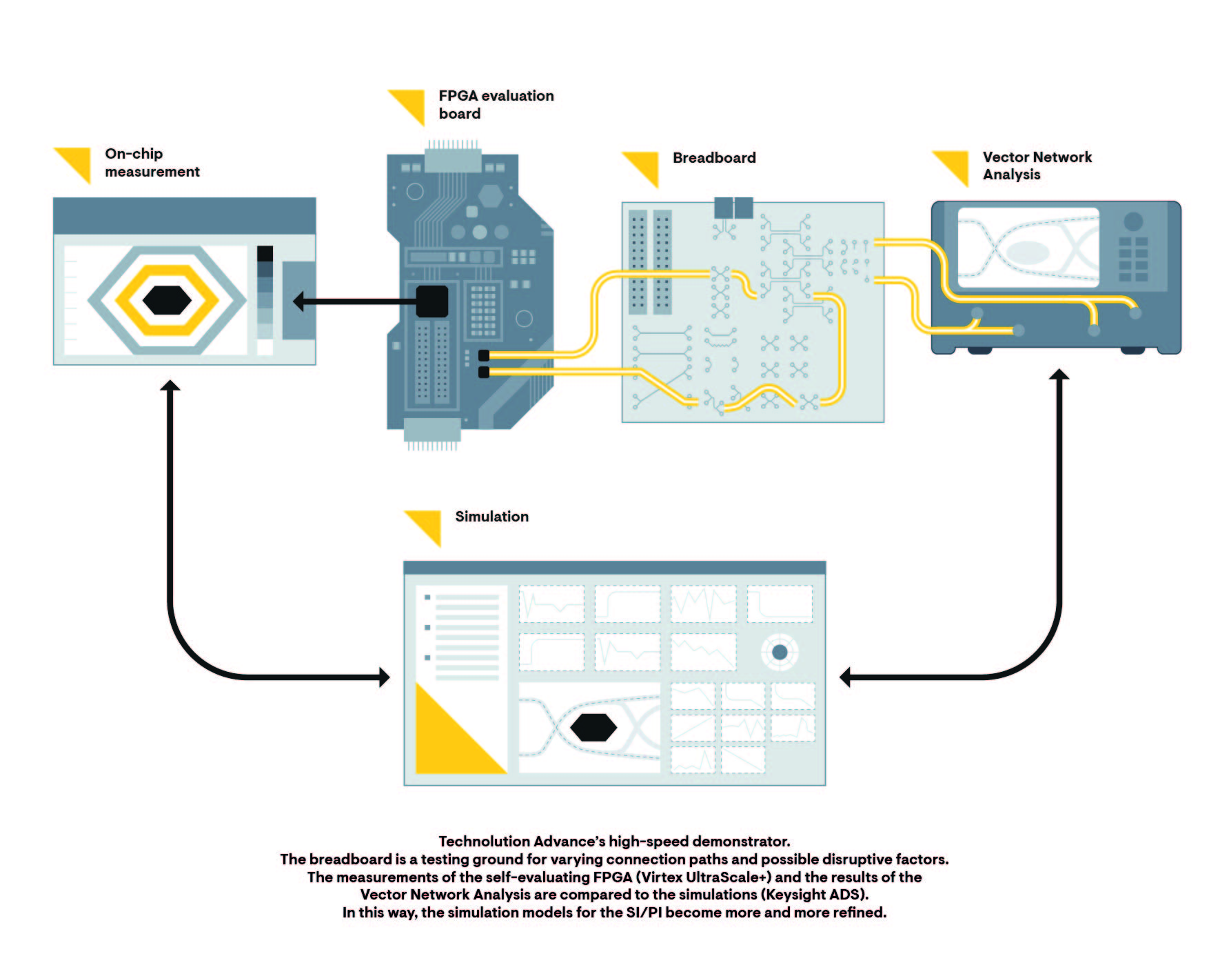
Simulations are one of the tools we use in our research of high-speed connections. They offer insight and make it possible to perform sensitivity analyses that can’t be done through measurement. A simulator can calculate the behavior of a circuit board and connectors based on Maxwell’s equations on electromagnetism. Models of chips determine whether bits arrive intact at their destination. Thanks to these simulations, we can decide pre-layout what the best architecture is and what type of material should be used. But we also use simulations post-layout, to check that the architecture that was realized still offers sufficient SI. We then measure to verify that our simulations include the correct physical factors, which means the simulations’ reliability is enhanced after each measurement.

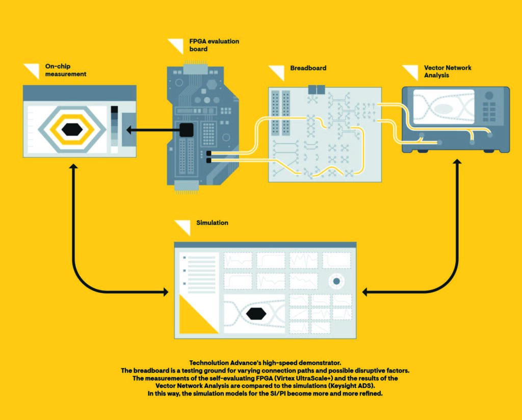
We develop demonstrator projects to thoroughly test the theory. One of the things we use to do this is an FPGA-based demonstrator that can transport up to 50 Gbit/s per lane. The FPGA can visualize the SI on the chip using an eye pattern. In addition, we’ve designed a breadboard, a large circuit board with almost 200 different structures whose impact on the SI we want to examine. The breadboard can be linked to the FPGA so that we can actually measure the end-to-end SI. If the simulation is correct, the eye pattern of the measurement will be identical to that of the simulation. This helps us define our best practices, which can then be deployed straightaway in projects for clients.
Right approach
As experts in high-speed electronics, FPGA development, embedded systems and application software, we develop medical, cryptographic and diagnostic systems for Ethernet, PCI Express, USB, DDR, HDMI and other serial high-speed interfaces. In our experience, it’s essential for any high-speed development project to give SI and PI the attention they require from the start, just like we do with electromagnetic compatibility and producibility. The right approach can make it possible to realize reliable electrical connections at terabit speeds – within time and budget. In the quest for very high speeds, we balance theoretical modeling with simulations on the one hand and a pragmatic, results-focused approach on the other. We’re keen to share our knowledge and experience in the field with clients and partners, in a context of co-creation that spans the entire development path. From the first back-of-the-envelope calculations to determining the compliance testing strategy for complex devices with high-speed data connections
